
Applied Physics Laboratory
Department of Physics, B.M.S. College of Engineering, Bengaluru
APPLIED PHYSICS PRACTICAL
OBSERVATION AND DATA ENTRY BOOK
Academic year: 2023 – 2024 onwards
Name of the student
Roll No./USN
Section, Batch
Branch
Cluster
Faculty in-charge
Department of Physics
B.M.S. College of Engineering
Bull Temple Road, Bengaluru-560019
http://www.bmsce.ac.in/home/Physics-Department-About


Applied Physics Laboratory
Department of Physics, B.M.S. College of Engineering, Bengaluru
LIST OF EXPERIMENTS FOR COMPUTER SCIENCE / ELECTRICAL / MECHANICAL
CLUSTER
Sl.
No.
Experiment
Page
Date
Marks
Signature of the
Faculty
1
Wavelength of LASER beam by diffraction
2
2
Divergence angle of a LASER beam
4
3
Numerical aperture of an optical fiber
6
4
Wavelength of transparent LEDs
8
5
Fermi energy of copper
12
6
Dielectric constant of a material by charging and
discharging of a capacitor
16
7
Series resonance in LCR circuits
20
8
Parallel resonance in LCR circuits
22
COMPUTER SCEINCE / ELECTRICAL CLUSTER
9
V-I characteristics of a photodiode
24
10
Energy gap of a semiconductor using four probe
method
26
MECHANICAL CLUSTER
9
Thermal conductivity of a metal by Forbe’s
method
30
10
Thermal conductivity of a poor conductor by Lee
Charlton’s method
34
CIVIL CLUSTER
9
Spring constant of a given spring
38
10
Analysis of X-ray diffractogram
48
Total Marks Scored

Applied Physics Laboratory
Department of Physics, B.M.S. College of Engineering, Bengaluru

Applied Physics Laboratory
Department of Physics, B.M.S. College of Engineering, Bengaluru
General instruction to student:
1. Submission of manual and record in every class for evaluation is mandatory.
2. Entries of observations should be made in manual only in blue pen.
3. Calculations and substitutions should be shown explicitly.
4. After completion of the experiment, student should switch off the instruments and
disconnect the circuit.
5. The record book should be written following the format given in the manual.
6. Transfer the readings to the record book only after the evaluation by faculty in-charge in the
manual.
7. An additional graph should be drawn and attached to the record.
8. Mobile phones and smart watches are not allowed to the lab.
9. The student should bring his/her own calculator (except programmable calculator), pen,
pencil, eraser, etc., borrowing the same from others is not permitted.
Safety precautions about LASER:
Students are advised:
➢ Not to look at the LASER beam directly as it is hazardous to eyes
➢ To conduct the experiment only in the presence of faculty
➢ To switch OFF LASER source immediately after the completion of experiment
➢ Not to play with the LASER beam

Applied Physics Laboratory
Department of Physics, B.M.S. College of Engineering, Bengaluru Page 1
Schematic Diagram:
Observations:
Distance between grating and the screen, d = ________ m
The number of rulings per inch on the grating, N = ________
Tabular column:
For LASER - 1
Order of
diffraction
n
Distance of the spot from the
centre in m
sin θ
λ nm
Left
Right
Mean (x)
1
2
3
4
Mean,
1
=
For LASER - 2
Order of
diffraction
n
Distance of the spot from the
centre in m
sin θ
λ nm
Left
Right
Mean (x)
1
2
3
4
Mean,
2
=
Error Analysis:
The formula for error analysis is given by:
100% x
valueExpected
valueExpectedvaluealExperiment
Error
−
=

Applied Physics Laboratory
Department of Physics, B.M.S. College of Engineering, Bengaluru Page 2
Experiment No. Date:
WAVELENGTH OF LASER BEAM BY DIFFRACTION
Aim: To determine the wavelength of the given laser source.
Apparatus: Diode laser source, optical bench, moveable stand and screen and metre scale.
Formula:
1. The wavelength, λ of the laser beam is given by
where, θ is the angle of diffraction
n is the order of diffraction
N is the number of rulings on the grating per inch
2. The angle of diffraction θ is given by
where, x is the distance between the central spot and the spot of n
th
order
d is the distance of the screen from the grating.
Procedure:
1. Note down the distance d between the grating and the screen. Mount the laser source at one end
of the optical bench.
2. Mount the directional pointer on another stand of the optical bench.
3. Arrange the laser beam to touch the pointer for horizontal alignment of the optical bench.
4. Remove the pointer and mount the grating on that stand to get the diffraction pattern on the
screen.
5. Attach a graph sheet on the screen and mark the central maxima and at least four orders of the
diffraction pattern on either side of the central maxima on it.
Result:
The wavelength of the given laser source is found to be λ
1
= .................nm and λ
2
= .................nm.

Applied Physics Laboratory
Department of Physics, B.M.S. College of Engineering, Bengaluru Page 3
Schematic Diagram:
Tabular Column:
For LASER - 1
Spot
No
Distance ‘d’
in m
Horizontal
Diameter (w
h
)
in m
Vertical
Diameter (w
v
)
in m
Mean diameter (m)
+
=
2
vh
ww
w
=
−
d
w
2
tan
1
I
II
III
Average θ
1
=
For LASER - 2
Spot
No
Distance ‘d’
in m
Horizontal
Diameter (w
h
)
in m
Vertical
Diameter (w
v
)
in m
Mean diameter (m)
+
=
2
vh
ww
w
=
−
d
w
2
tan
1
I
II
III
Average θ
2
=
Error Analysis:
The formula for error analysis is given by:
Substitution & Calculation:
100% x
valueExpected
valueExpectedvaluealExperiment
Error
−
=

Applied Physics Laboratory
Department of Physics, B.M.S. College of Engineering, Bengaluru Page 4
Experiment No. Date:
DIVERGENCE ANGLE OF A LASER BEAM
Aim: To determine the half angle of divergence of the given laser beam.
Definition: Divergence of a laser beam is defined as its spread with distance. It is measured in
terms of angle subtended by the laser spot at the point of origin of the laser beam.
Apparatus: Diode laser source, optical bench, moveable stand and screen and metre scale.
Formula: The half angle of divergence θ of the laser beam is given by
=
−
d
w
2
tan
1
where, w is the mean diameter of the laser spot
d is the distance of the screen from the source.
Procedure:
1. Mount the laser source at the one end of the optical bench.
2. Mount the directional pointer on the other end of the optical bench.
3. Arrange the laser beam to touch the pointer for horizontal alignment of the optical bench and
then remove the pointer.
4. Now place the moveable stand and screen at distance d
1
and note down the horizontal and
vertical diameters of the spot.
5. Repeat the above step for two more distances.
Result: The half angle of divergence of given LASER beam is found to be θ
1
= ......................deg.,
and θ
2
= ......................deg.

Applied Physics Laboratory
Department of Physics, B.M.S. College of Engineering, Bengaluru Page 5
Schematic Diagram:
Tabular column:
Cable
Spot diameter
D (mm)
Distance
f (mm)
f
D
2
tan =
θ
Sin (θ
Average
)
Cable 1
Average θ
Cable 2
Average θ
Substitution & Calculation:
Error Analysis:
The formula for error analysis is given by:
100% x
valueExpected
valueExpectedvaluealExperiment
Error
−
=
sin=NA

Applied Physics Laboratory
Department of Physics, B.M.S. College of Engineering, Bengaluru Page 6
Experiment No. Date:
NUMERICAL APERTURE OF AN OPTICAL FIBER
Aim: To determine the numerical apertures of the given two optical fibers.
Apparatus: Laser source, optical fiber cables, screen, transverse motion bench and relative
intensity meter.
Formula: The numerical aperture (NA) of an optical fiber is given by
where, θ is acceptance angle of the fiber.
Procedure:
1. Connect one end of the optical fiber cable (OFC) to the LASER source and the other end to the
connector which slides on the transverse motion bench.
2. Slide the connector close to the graduated screen (every line is 2 mm apart), fixed at the end of
the transverse motion bench and note down the spot diameter and the distance between the OFC
connector and the screen.
3. Move the connector to four more different distances from the screen and note down the spot
diameter each time.
4. Disconnect the cable from slide motion bench and connect it to the relative intensity meter and
note down the reading.
5. Repeat the experiment for the second cable.
6. Plot the graph of distance between the source (OFC connector) and the spot diameter.
Result: The numerical apertures of the given two optical fiber cables are:
------------- for cable 1 and ------------- for cable 2.
sin=NA

Applied Physics Laboratory
Department of Physics, B.M.S. College of Engineering, Bengaluru Page 7
Circuit diagram:
Expected Graph:
Tabular column:
Applied
Voltage
in volts
LED 1
LED 2
Colour:
Colour:
Voltage across
LED (V)
Current
I (mA)
Voltage
across
LED (V)
Current
I (mA)
0.2
0.4
0.6
0.8
1.0
1.2
1.4
1.6
1.8
2.0
2.2
2.4
2.6
2.8
3.0
3.2
3.4
3.6

Applied Physics Laboratory
Department of Physics, B.M.S. College of Engineering, Bengaluru Page 8
Experiment No. Date:
WAVELENGTH OF TRANSPARANT LED
Aim: To determine the wavelengths of the given light emitting diodes (LEDs).
Apparatus: 0-5 V Power supply, LED s, 330 Ω resistor, 0-5 V Voltmeter, DC milliammeter.
Principle: Energy quantization
Formula: The wavelength of LED is calculated using the relation,
Where, h is Planck’s constant = 6.63 x 10
-34
Js
c is speed of light = 3 x 10
8
m s
-1
e is electron charge = 1.602 x 10
-19
C
V is the knee voltage in volts of the LED, (to be measured from graph).
Procedure:
1. Connect the circuit as shown in the figure, with a 5 volts supply, 330 Ω resistor, milliammeter
and an LED connected in series and a voltmeter connected in parallel to LED.
2. Increase the voltage of the source in steps of 0.2 V using fine adjustment knob. Note down the
voltage across the LED and the current through the LED.
3. Repeat the above steps for another LED.
4. Plot the V-I characteristics on a graph sheet.
5. Mark the voltage at which non-zero current is registered. Draw a tangent to the curve at that
point. Project it to voltage axis. Read the voltage at the intersection which is the knee voltage.
6. Calculate the wavelength of given LEDs using the above formula.

Applied Physics Laboratory
Department of Physics, B.M.S. College of Engineering, Bengaluru Page 9
Substitution & Calculation:
Knee voltage for LED 1 = ___________ V (From graph)
Knee voltage for LED 2 = ___________ V (From graph)
Error Analysis:
The formula for error analysis is given by:
100% x
valueExpected
valueExpectedvaluealExperiment
Error
−
=

Applied Physics Laboratory
Department of Physics, B.M.S. College of Engineering, Bengaluru Page 10
Result:
1. The wavelength of given LED 1, λ
1
= _______________ m
2. The wavelength of given LED 2, λ
2
= _______________ m

Applied Physics Laboratory
Department of Physics, B.M.S. College of Engineering, Bengaluru Page 11
Circuit Diagram:
Observations:
Free electron concentration of copper,
n
= 8.45 x10
28
/m
3
Charge of the electron,
e
= 1.6 x 10
-19
C
Radius of the given copper wire,
r
= 0.14 x10
-3
m
Mean Free Path of electrons
λ
= 39 x 10
-9
m
The length of the copper wire,
l
= 10 m
Mass of the electron
m
= 9.1 x 10
-31
kg
Temperature
T
= 300 K
The resistance per unit length of the bridge wire,
ρ
= 0.032 Ω cm
-1
The dial resistance,
R
d
= ___

Applied Physics Laboratory
Department of Physics, B.M.S. College of Engineering, Bengaluru Page 12
Experiment No:
Date:
FERMI ENERGY OF COPPER
Aim: To determine the Fermi energy of copper.
Apparatus: Copper coil, oil/water bath, thermometer, Callender - Griffith’s bridge, galvanometer,
power supply
Formula: The Fermi energy of copper is given by
where,
n
is the free electron concentration of copper in /m
3
e
is charge of the electron in C
r
is the radius of the given copper wire in m
λ
is the mean free path of electron inside the copper at RT in m
l
is the length of the copper wire in m
T
is the room temperature in K
R/T
is the mean resistance per unit temperature calculated from the experiment
in Ω/K
Procedure:
1. A copper wire of given length is wound on a fiber sheet in the form of a coil.
2. This coil is immersed in water bath and is connected to one arm of a Callender-Griffith’s bridge
(the S arm). A compensating wire is connected to the opposite arm (the R arm).
3. Now adjust the standard resistance dial to 1 ohm. Set the voltage output of the power supply to
1 V. Slide the key along the bridge and obtain null deflection. Note down balancing length ‘x’
in cm.
4. Obtain the balancing lengths at various temperatures. Tabulate the results.

Applied Physics Laboratory
Department of Physics, B.M.S. College of Engineering, Bengaluru Page 13
Tabular column:
Sl.
No.
Temp
0
C
Temp
K
‘x’
in cm
R = R
d
+ x ρ in Ω
[R/T] in Ω/K
1
RT =
2
80
353
3
75
348
4
70
343
5
65
338
6
60
333
Mean [R/T] =
Substitution & Calculation:

Applied Physics Laboratory
Department of Physics, B.M.S. College of Engineering, Bengaluru Page 14
Error Analysis:
The formula for error analysis is given by:
Result:
The Fermi energy E
F
of copper = J = eV.
100% x
valueExpected
valueExpectedvaluealExperiment
Error
−
=

Applied Physics Laboratory
Department of Physics, B.M.S. College of Engineering, Bengaluru Page 15
Circuit Diagram:
Expected graph:
Observations:
Thickness of the dielectric material,
d =
70x10
-6
m
Area of cross section of the dielectric material
A =
57.4 x 10
-4
m
2
Time taken for charging /discharging to 1/e of the voltage value
T
½
=
________ s
Resistance connected in the circuit
R =
1x 10
4
Ω
Permittivity of free space
ε
o
=
8.85 x 10
-12
F/m

Applied Physics Laboratory
Department of Physics, B.M.S. College of Engineering, Bengaluru Page 16
Experiment No. Date:
DIELECTRIC CONSTANT OF A MATERIAL BY CHARGING
AND DISCHARGING OF A CAPACITOR
Aim: To determine the dielectric constant of the material by the method of charging and
discharging of the capacitor.
Apparatus: Capacitor with known dimensions, 5 V DC power supply, voltmeter, resistor, stop
clock.
Formula: The dielectric constant k of the material inside the capacitor is
where,
d
is the thickness of the dielectric material in m
A
is the area of cross section of the dielectric material in m
2
T
1/2
is the time taken for charging /discharging to rise/fall to 1/e times of the
initial value of voltage in seconds
R
is the resistance connected in the circuit in Ω
ε
o
is permittivity of free space is 8.85x10
-12
F/m
Procedure:
1. Connect the circuit as shown and discharge the capacitance fully so that the voltmeter reads
zero volts.
2. Switch on the power supply and stop clock simultaneously.
3. Note down the voltage across the capacitor at 10 s intervals up to 150 s.
4. Reset the stop clock. Now switch off the power supply and start the stop clock
simultaneously.
5. Again, note down the voltage across the capacitor at 10 s intervals.
6. Plot a graph of voltage across the capacitor and time both while charging and discharging.
Find T
1/2
.

Applied Physics Laboratory
Department of Physics, B.M.S. College of Engineering, Bengaluru Page 17
Tabular column:
Time
in seconds
Voltage across capacitor in V
Charging Mode
Discharging Mode
0
0
10
20
30
40
50
60
70
80
90
100
110
120
130
140
150

Applied Physics Laboratory
Department of Physics, B.M.S. College of Engineering, Bengaluru Page 18
Substitution & Calculation:
Error Analysis:
The formula for error analysis is given by:
Result: The dielectric constant of the material present between the plates of the capacitor is,
k = ___________
100% x
valueExpected
valueExpectedvaluealExperiment
Error
−
=

Applied Physics Laboratory
Department of Physics, B.M.S. College of Engineering, Bengaluru Page 19
Circuit Diagram:
Frequency response curve:
Observation:
Capacitance of the given capacitor, C = ______ μF
Series Circuit
Substitution & Calculation:
Error Analysis:
The formula for error analysis is given by:
Frequency
(Hz)
Current
(mA)
Frequency
(Hz)
Current
(mA)
200
950
300
1000
400
1050
450
1100
500
1150
550
1200
600
1250
650
1300
700
1350
750
1400
800
1500
850
1600
900
Cf
L
r
22
4
1
=
100% x
valueExpected
valueExpectedvaluealExperiment
Error
−
=

Applied Physics Laboratory
Department of Physics, B.M.S. College of Engineering, Bengaluru Page 20
Experiment No. Date:
SERIES RESONANCE IN LCR CIRCUIT
Aim: 1. To study the frequency response of the series resonance circuits.
2. To determine the unknown value of the given inductor, bandwidth and quality factor for
the series resonance circuits.
Apparatus: Audio frequency generator, resistor, inductor, capacitor and milliammeter.
Formula:
i. The value of inductance
H
➢ f
r
is resonant frequency in Hz
➢ C is the capacitance in F
ii. The band width
= (f
1
~ f
2
) in Hz
➢ f
1
and f
2
are lower and upper cut-
off frequencies respectively in
Hz
iii. The quality factor of the circuit
Procedure:
1. Connect a signal generator, a resistor, an a.c. milliammeter, an inductor and a capacitor in
series.
2. Switch on the signal generator and adjust its amplitude knob to get the milliammeter readings
within the scale for all frequencies between 200 to 1200 Hz.
3. Increase the frequency in steps of 50 Hz up to 1200 Hz starting from 200 Hz and note down the
milliammeter readings.
4. Perform the calculations for the observations of series LCR circuit.
Results:
The resonant frequency of series LCR circuit
=
________________________
Hz
The bandwidth of the series LCR circuit
=
________________________
Hz
The quality factor of the series LCR circuit
=
________________________
The value of the inductance of the coil L
=
________________________
H

Applied Physics Laboratory
Department of Physics, B.M.S. College of Engineering, Bengaluru Page 21
Circuit Diagram:
Frequency response curve:
Observation:
➢ Capacitance of the given capacitor, C = ______ μF
Parallel Circuit
Substitution & Calculation:
Error Analysis:
The formula for error analysis is given by:
Frequency
(Hz)
Current
(mA)
Frequency
(Hz)
Current
(mA)
200
950
300
1000
400
1050
450
1100
500
1150
550
1200
600
1250
650
1300
700
1350
750
1400
800
1500
850
1600
900
Cf
L
r
22
4
1
=
100% x
valueExpected
valueExpectedvaluealExperiment
Error
−
=

Applied Physics Laboratory
Department of Physics, B.M.S. College of Engineering, Bengaluru Page 22
Experiment No. Date:
PARALLEL RESONANCE IN LCR CIRCUITS
Aim: 1. To study the frequency response of the parallel resonance circuits.
2. To determine the unknown value of the given inductor, bandwidth and quality factor for
the parallel resonance circuits.
Apparatus: Audio frequency generator, resistor, inductor, capacitor and milliammeter.
Formula:
i. The value of inductance
H
➢ f
r
is resonant frequency in Hz
➢ C is the capacitance in F
ii. The band width
= (f
1
~ f
2
) in Hz
➢ f
1
and f
2
are lower and upper cut-
off frequencies respectively in
Hz
iii. The quality factor of the circuit
Procedure:
1. Connect a signal generator, a resistor, an a.c. milliammeter, an inductor and a capacitor in
parallel.
2. Switch on the signal generator and adjust its amplitude knob to get the milliammeter readings
within the scale for all frequencies between 200 to 1200 Hz.
3. Increase the frequency in steps of 50 Hz up to 1200 Hz starting from 200 Hz and note down the
milliammeter readings.
4. Perform the calculations for the observations of parallel LCR circuit.
Results:
The resonant frequency of parallel LCR circuit
=
________________________
Hz
The bandwidth of the parallel LCR circuit
=
________________________
Hz
The quality factor of the parallel LCR circuit
=
________________________
The value of the inductance of the coil L
=
________________________
H

Applied Physics Laboratory
Department of Physics, B.M.S. College of Engineering, Bengaluru Page 23
Circuit Diagram:
Graph:
Tabular column:
Voltage (V)
Current (mA)
Distance between LED
& Photodiode = 1 cm
Distance between LED &
Photodiode = 2 cm
Distance between LED &
Photodiode = 3 cm
0
1
2
3
4
5
6
7
8

Applied Physics Laboratory
Department of Physics, B.M.S. College of Engineering, Bengaluru Page 24
Experiment No. Date:
PHOTODIODE
Aim: To study the I-V characteristics of the given photo diode and determine the reverse
resistance.
Apparatus: 0-5 V regulated power supply, 0-5 mA digital DC ammeter, 0-20 V digital DC volt
meter, white light LED and Ga-As photo diode.
Formula:
Experimental procedure:
1. The LED (white light) and photodiode (PD) are placed face to face.
2. Photo Diode is connected in reverse biased mode.
3. LED power is set to 10 mW by turning the knob to its minimum position.
4. After ensuring that the LED is glowing and Photo Diode is covered with a cloth, the current is
noted.
5. The distance between LED and PD is set to 1cm.
6. Voltage across the photo diode VPD is varied and the corresponding current IPD is noted.
7. Experiment is repeated for different distances between LED and PD and the readings are
tabulated.
8. A graph showing the variation of VPD on x-axis and IPD on y-axis is drawn as shown in
model graph.
Result:
It is observed from the graph that there are different curves for different light intensities. The equal
spacing between characteristic curves indicates linearity of photo current with light intensity.
The reverse resistance is found to be = …....................….. Ω

Applied Physics Laboratory
Department of Physics, B.M.S. College of Engineering, Bengaluru Page 25
Schematic diagram:
Expected graph:

Applied Physics Laboratory
Department of Physics, B.M.S. College of Engineering, Bengaluru Page 26
Experiment No: Date:
ENERGY BAND GAP OF A SEMICONDUCTOR BY FOUR
PROBE METHOD
Aim: To study the temperature dependence of resistivity and to determine the energy gap of a
semiconductor.
Apparatus: Semiconductor in the form of a crystal, thermometer, four probes apparatus
Formula: The resistivity of the material of the crystal is given by
where, R is the resistance of the crystal in ohm,
A is area of the crystal in m
2
l is the length of the crystal in m.
Energy gap of the semiconductor is given by
where, k is Boltzmann constant =1.38x10
-23
J/K
Slope is calculated from the graph of log
10
R vs (1/T)
Procedure:
1. Connect the circuit as in diagram.
2. Immerse the thermistor in the port in the crystal holder of the four probes apparatus.
3. Adjust the current at 2.00 mA. This value of current should be kept constant.
4. Switch on the oven and heat the sample up to 200
o
C.
5. Switch off the oven and allow the crystal to cool.
6. Note down the value of voltage for every 10
o
C fall in temperature starting from 200
o
C.
7. Plot a graph of ρ versus T.
8. Plot another graph of log
10
R versus (1/T) and calculate its slope.
eV
10602.1
2303.2
19
=
−
Slopek
E
g

Applied Physics Laboratory
Department of Physics, B.M.S. College of Engineering, Bengaluru Page 27
Observation:
Current, I = 2.00 mA
Area of the crystal, A = 3.75x10
-6
m
2
Length of the crystal, l = 2x10
-3
m
Tabular column:
Sl.
No.
Temp
°C
Temp T,
K
Voltage
mV
Resistance
Ω
Resistivity
Ω-m
[(1/T) x 10
-3
]
K
-1
log
10
R
1
160
433
2.309
2
150
423
2.364
3
140
413
2.421
4
130
403
2.481
5
120
393
2.544
6
110
383
2.610
7
100
373
2.680
8
90
363
2.755
9
80
353
2.833
10
70
343
2.915
Applied Physics Laboratory
Department of Physics, B.M.S. College of Engineering, Bengaluru Page 28
Substitution & Calculation:
Error Analysis:
The formula for error analysis is given by:
Result:
The temperature dependence of the resistivity of the given semiconductor is studied.
The energy gap of the given semiconducting material is E
g
= ………….. eV
100% x
valueExpected
valueExpectedvaluealExperiment
Error
−
=
eV
10602.1
2303.2
19
=
−
Slopek
E
g

Applied Physics Laboratory
Department of Physics, B.M.S. College of Engineering, Bengaluru Page 29
Experimental setup:
Expected graph:
Observations:
Tabular column 1:
Distance
(m)
x
1
5 x 10
-2
m
x
2
10 x 10
-2
m
x
3
15 x 10
-2
m
x
4
20 x 10
-2
m
x
5
25 x 10
-2
m
x
6
30 x 10
-2
m
Steady
temperature
T in °C
Temp & Timer
module
Heating
Element
Temperature Sensors
T
1
T
2
T
3
T
4
T
5
T
6
X
1
=5cm
X
2
=10cm
X
2
=15cm
X
3
=20cm
X
4
=25cm
X
5
=30cm

Applied Physics Laboratory
Department of Physics, B.M.S. College of Engineering, Bengaluru Page 30
Experiment No: Date:
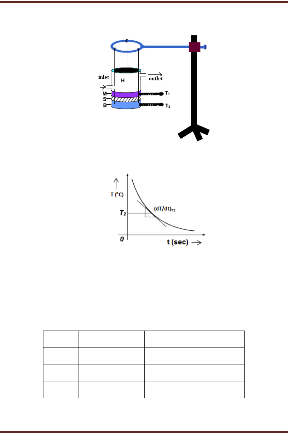
THERMAL CONDUCTIVITY OF A METAL BY FORBE’S
METHOD
Aim: To measure the thermal conductivity of a good conductor by Forbe’s method.
Apparatus: A long uniform hollow metal rod with holes drilled at appropriate places with
semiconductor thermometers (six), temperature and time reading unit.
Formula: The coefficient of thermal conductivity of the metal rod is given by
where,
ρ
is the density of the metal rod in kg/m
3
s
is its specific heat J/kg.K
[ΔT/Δt]
is rate of change of temperature
[dT/dx]
is temperature gradient [(T
2
-T
5
)/(x
5
-x
2
)]
Procedure:
2. Insert the heating element into open end of the hollow metal rod. Heat the rod for about half an
hour so as to attain steady state.
3. Connect the output of the thermometers to the temperature and timer module.
4. Note down the temperature at different distances x as in tabular column 1. Plot a graph T vs X.
5. Find the ratio [(T
2
-T
5
)/(x
5
-x
2
)] from the graph.
6. Now turn off the heating. Reset the timer. Note down the temperature of all six thermometers at
an interval of two minutes, up to ten minutes as in tabular column 2.
7. Calculate ∆T = [T
@ 0s
~ T
@ 600s
] and consider ∆t = 600 s. Compute the sum
x
t
T
L
0
as
indicated in tabular column 2.
Applied Physics Laboratory
Department of Physics, B.M.S. College of Engineering, Bengaluru Page 31
Observations:
Density of the material (brass or iron) of the rod, ρ = 8520 or 7850 kg/m
3
Specific heat of the material (brass or iron) of the rod s = 401.93 or 452 J/kg K
Tabular column 2:
Temp. ⁰C
Time t (sec)
x
cm
∆x
m
0
120
240
360
480
600
T
1
(at x
1
)
5
0.05
T
2
(at x
2
)
10
0.05
T
3
(at x
3
)
15
0.05
T
4
(at x
4
)
20
0.05
T
5
(at x
5
)
25
0.05
T
6
(at x
6
)
30
0.05
x
t
T
L
0

Applied Physics Laboratory
Department of Physics, B.M.S. College of Engineering, Bengaluru Page 32
Substitution & Calculation:
x
t
T
L
0
from the tabular column =
, the temperature gradient from the graph =
Error Analysis:
The formula for error analysis is given by:
Result: The thermal conductivity of the given good conductor is = ………………..W/mk
100% x
valueExpected
valueExpectedvaluealExperiment
Error
−
=
Applied Physics Laboratory
Department of Physics, B.M.S. College of Engineering, Bengaluru Page 33
Experimental Setup:
Expected Graph:
Observations:
Thickness of a poor conductor using screw gauge:
Zero error (ZE) = Zero Correction (ZC) =
Least count (LC) = _________________mm
Trial No.
PSR
HSR
TR=PSR+{(HSR-ZE)×LC} mm
1
2
3
Thickness of a poor conductor = ……………mm = …………………. m

Applied Physics Laboratory
Department of Physics, B.M.S. College of Engineering, Bengaluru Page 34
Experiment No:
Date:
THERMAL CONDUCTIVITY OF A POOR CONDUCTOR BY
LEE AND CHARLTON’S METHOD
Aim: To determine the thermal conductivity of given poor conductor by Lee and Charlton’s
method.
Apparatus: Lee and Charlton’s apparatus, poor conductor in the form of a disc, stop clock, Vernier
callipers, screw gauge, two thermometers, steam generator and balance.
Formula: The thermal conductivity of a poor conductor is calculated using the relation,
where,
m
is mass of the metallic disc B in kg
s
is specific heat of the material of B in J/kg.K
d
is thickness of the poor conductor S in m
r
is radius of the poor conductor S in m
T
1
is steady temperature of disc M in ⁰C
T
2
is steady temperature of disc B in ⁰C
h
is height of the metallic disc B in m
dT/dt
is rate of cooling as calculated from the graph
Procedure:
1. Measure the diameter and hence the radius, r of the poor conducting specimen S, using a scale.
2. Measure the thickness, d of the sample using a screw gauge.
3. Arrange the steel disc, poor conductor and steam chamber as shown in the schematic diagram.
Insert the thermometers into the grooves of steam chamber and steel disc, which measure the
temperatures T
1
and T
2
, respectively.
4. Turn on the heater and monitor the temperatures T
1
and T
2
at a regular interval till they reach
the steady state. Note the steady state temperatures T
1
and T
2
.
5. To determine the rate of cooling of brass disc, lift the heating chamber and remove the
sample disc S, then place the heating chamber directly on the brass disc, B.
6. Allow the brass disc B to heat at least about 10
0
C above the steady state temperature T
2
measured in the first part of the experiment. Remove the heating chamber.

Applied Physics Laboratory
Department of Physics, B.M.S. College of Engineering, Bengaluru Page 35
Observation:
Mass of the metallic disc B, m = 0.93 kg
Specific heat of the material of B, s = 520 J/kg K
Thickness of the poor conductor, d = _______ m
Radius of the poor conductor S, r = _______ m
Steady temperature of disc M, T
1
= ______ ⁰C
Steady temperature of disc B, T
2
= ______ ⁰C
Height of the metallic disc B, h = 0.01 m
Tabular column:
Rate of cooling of brass disc:
Sl. No.
Time (min)
Time in s
Temperature of
steel disc T ⁰C
1
0
0
2
1
60
3
2
120
4
3
180
5
4
240
6
5
300
7
6
360
8
7
420
9
8
480
10
9
540
11
10
600

Applied Physics Laboratory
Department of Physics, B.M.S. College of Engineering, Bengaluru Page 36
7. Switch on the stop clock and measure the temperature of brass disc at an interval of 60 s as it
cools down.
8. Plot a graph of temperature T of brass disc as a function of time. Draw tangential line to the
curve, corresponding to the temperature T
2
and determine its slope. The slope is equivalent to
9. Calculate the thermal conductivity, K using the given formula.
Substitution & Calculation:
Rate of cooling from the calculated graph [dT/dt] =
Error Analysis:
The formula for error analysis is given by:
=
Result:
Thermal conductivity of the given poor conductor specimen is found to be _________ W/mK.
100% x
valueExpected
valueExpectedvaluealExperiment
Error
−
=

Applied Physics Laboratory
Department of Physics, B.M.S. College of Engineering, Bengaluru Page 37
Experimental Setup:
Frequency response of the spring – mass system.
Tabular column 1:
Sl. No
Mass in g
Vibrating force
F = (m x g) kg m/s
2
Displacement (m)
1
w
2
w+50
3
w+100
4
w+150
5
w+200

Applied Physics Laboratory
Department of Physics, B.M.S. College of Engineering, Bengaluru Page 38
Experiment No. Date:
SPRING CONSTANT OF A GIVEN SPRING
Aim: (i) To find the spring constant of the given spring by oscillating it freely.
(ii) To draw the frequency response curve for forced oscillations.
Apparatus: A spring, a rod carrying weights and a stopper disc, channel, magnetic scale, drive
wheel, frequency oscillator, acrylic cylinder with water and a black lid.
Formula: The spring constant of the given spring
where, is the Slope of the straight line graph of restoring force F vs displacement x.
Procedure:
1. Hang the spring rod assembly from the fixed support and adjust the magnetic scale such that
the lower edge of the disc aligns with the zero mark.
2. Attach a 50 g weight to the rod and measure the distance through which the disc moves using
the magnetic scale.
3. Every time attach 50 g and note down the displacements for 100 g, 150 g and 200 g.
4. Plot a Force vs displacement graph and calculate the slope, of the straight line.
5. Total mass of the rod (m
rod
) and that of the spring (m
s
) is calculated as (m
rod
+ m
s
/3) and found
to be 25 g.
6. Attach the free end of the spring to one end of the thread and pass it over the pulley while the
other end is connected to the drive wheel whose frequency can be varied.
7. Unscrew the disc attached to the rod, pass it through the black lid of the acrylic cylinder.
Attach a 100 g weight and screw back the disc to the rod.
8. Fill the cylinder with water just below the brim and close the black lid.
9. Set the driving wheel’s frequency to 0.2 Hz and measure the total displacement of the disc by
aligning the magnetic scale suitably. Half of this value gives the amplitude.
10. Increase the frequency of the drive wheel in steps of 0.2 Hz and note down the displacements
up to 3 Hz

Applied Physics Laboratory
Department of Physics, B.M.S. College of Engineering, Bengaluru Page 39
Tabular column 2:
Amplitude of vibration for 100 g for various forced frequencies:
Sl. No
Frequency
(Hz)
Angular frequency
ω = (2πf) in s
-1
Displacement (m)
Amplitude (m)
1
0.2
2
0.4
3
0.6
4
0.8
5
1.0
6
1.2
7
1.4
8
1.6
9
1.8
10
2.0
11
2.2
12
2.4
13
2.6
14
2.8
15
3.0

Applied Physics Laboratory
Department of Physics, B.M.S. College of Engineering, Bengaluru Page 40
Substitution & Calculation:
Error Analysis:
The formula for error analysis is given by:
Result:
i. The spring constant of the given spring, k = ______________
ii. The frequency response curve for the given spring – mass system acted upon by external
drive wheel is drawn and the resonance frequency is found to be at ___________ Hz.
100% x
valueExpected
valueExpectedvaluealExperiment
Error
−
=

Applied Physics Laboratory
Department of Physics, B.M.S. College of Engineering, Bengaluru Page 41
Diagram:
FILM STRIP
Observations:
Wavelength of X-ray, = 1.54 x 10
-10
m
Tabular column:
Arc No.
TM reading
Arc
diameter
S = R ~ L
sin
Left
Right
MSR
CVD
TR (L)
MSR
CVD
TR (R)
5
4
3
2
1
Tr. No.
h, k, l
h
2
+k
2
+l
2
5
12
4
11
3
8
2
4
1
3
Mean a = ……………. m

Applied Physics Laboratory
Department of Physics, B.M.S. College of Engineering, Bengaluru Page 42
Experiment No:
Date:
ANALYSIS OF X-RAY DIFFRACTOGRAM
Aim: To calculate the Miller indices, inter-planar distance and lattice constant using the given
X-ray diffractogram for copper.
Apparatus: X-ray diffractogram and travelling microscope
Principle: A powder sample contains micro crystals having random orientations. When
monochromatic X-rays are incident on such a material, some of the orientations satisfy Bragg’s
condition for reflection . Since all the orientations are equally probable, the reflected
rays form a set of cones. When the irradiated powder specimen is surrounded by a cylindrical film,
the cones of reflected rays intersect the film in a series of concentric circular halves whose diameter
in mm is equal to 2 in degrees.
Formula:
where, is the wave length of X-rays used in m,
d is the inter-planar distance in m,
θ is the glancing angle
where, a is the lattice constant in m,
d is the inter-planar distance in m
{h k l} are the Miller indices of the
given plane
Procedure:
1. The given powder photograph fixed to a glass plate is taken.
2. The reading corresponding to each ring (starting from the extreme left or right) are noted using
traveling microscope
3. The values are tabulated. Miller indices, inter-planar distances and lattice parameter are found
using formulae given above.
Result:
1. Miller indices for different atomic planes are determined.
2. Inter-planar distances of different set of parallel planes are calculated.
3. Lattice constant a = ______________ m.
