
BMS Educational Trust (R)
BMS INSTITUTE OF TECHNOLOGY AND MANAGEMENT
Approved by AICTE, New Delhi, Affiliated to VTU, Belagavi, NAAC- A grade, Programs
are accreditated by NBA Avalahalli, Doddaballapur Road, Bengaluru-560 064
Tel: 080-2856 1576, fax: 2856 7186, web: https://bmsit.ac.in/
DEPARTMENT OF PHYSICS
ENGINEERING PHYSICS LABORATORY
MANUAL
I/II SEMESTER (CBCS SCHEME)
SUBJECT: ENGG. PHYSICS LAB
SUBJECT CODE: 18PHYL 16/26
PREPARED BY:
Staff members, Department of Physics,
BMSIT&M.
August- 2020

BMSIT&M Department of Physics Engineering Physics Lab manual August-2020
Page 2
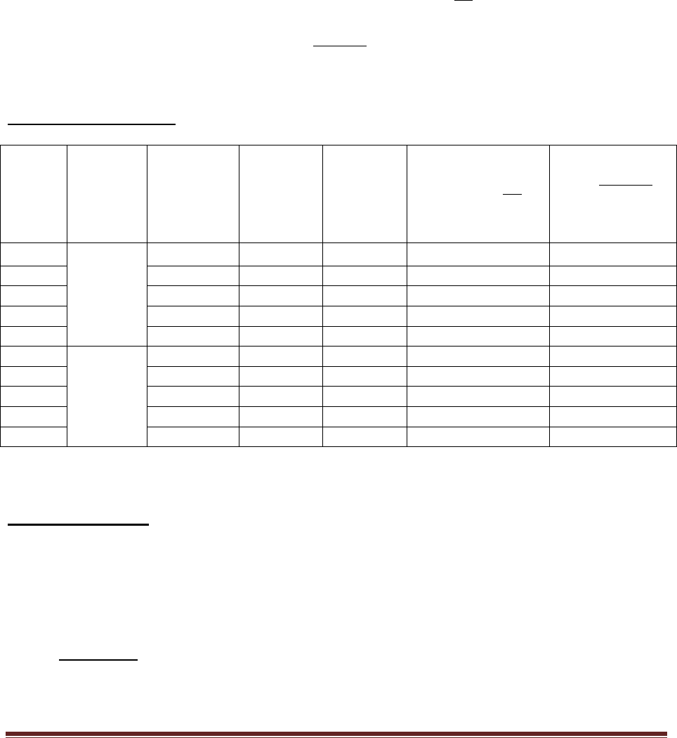
PERFORMANCE SHEET
NAME OF THE CANDIDATE:
SECTION: SEMESTER: I/II
ROLL NO/USN:
Max. Marks for each expt. 30
Sl.
No.
Name of the Experiment
Marks
Initial
of staff
1.
TORSIONAL PENDULUM
2.
TRANSISTOR CHARACTERISTICS
3.
FERMI ENERGY OF COPPER
4.
SERIES AND PARALLEL LCR
CIRCUITS
5.
NEWTON’S RINGS
6.
YOUNG’S MODULUS BY SINGLE
CANTILEVER
7.
DIELECTRIC CONSTANT
8.
LASER DIFFRACTION GRATING
9.
NUMERICAL APERTURE
10.
DETERMINATION OF SPRING
CONSTANT
11.
PHOTO DIODE
12.
MAGNETIC INTENSITY ALONG THE
AXIS OF A COIL
Signature of Batch in charge Signature of Head of the Dept.

BMSIT&M Department of Physics Engineering Physics Lab manual August-2020
Page 3
DEPARTMENT OF PHYSICS
DOs
Bring observation book, Lab manual & record book regularly.
Write the write up of the experiment in advance in the observation
book before coming to the practical class.
Bring calculator to the practical class regularly.
Handle the apparatus/equipment gently and carefully.
Return the apparatus collected, to lab instructor before leaving the
lab.
DON’Ts
Dumping your bag on the work table.
Giving your observation book and record books to others.
Forgetting to check your belongings before leaving the lab.
Spoiling of the apparatus/equipment as it is meant for your benefit
only.
Switch on electronic equipment before getting the approval by the
teacher/instructor.
Bringing mobile phones inside the Laboratory.
Instructions to students:
1. All calculations must be carried out using SI units.
2. All entries in the observation book should be done using pen only
3. Wherever graphs have to be plotted plotting has to be done using pencil only.

BMSIT&M Department of Physics Engineering Physics Lab manual August-2020
Page 4
CONTENTS
Sl.
No.
Name of the Experiment
Page No.
1.
TORSIONAL PENDULUM
5-8
2.
TRANSISTOR CHARACTERISTICS
9-11
3.
FERMI ENERGY OF COPPER
12-13
4.
SERIES AND PARALLEL LCR
CIRCUITS
14-17
5.
NEWTON’S RINGS
18-21
6.
YOUNG’S MODULUS BY SINGLE
CANTILEVER
22-24
7.
DIELECTRIC CONSTANT
25-26
8.
LASER DIFFRACTION GRATING
27-28
9.
NUMERICAL APERTURE
29-30
10.
DETERMINATION OF SPRING
CONSTANT
31-33
11.
PHOTO DIODE
34-36
12.
MAGNETIC INTENSITY ALONG
THE AXIS OF A COIL
37-38
Viva-voce questions
39-41

BMSIT&M Department of Physics Engineering Physics Lab manual August-2020
Page 5
1. TORSIONAL PENDULUM
AIM: To determine the moment of inertia of an irregular body and to calculate the rigidity
modulus of the material by the principle of torsional pendulum.
FORMULA:
Moment of Inertia of an irregular body is given by
2
0
2
0
T
T
I
I
mean
kgm
2
(1)
Where I
0
is the moment of Inertia of an irregular body in kg.m
2
I is the moment of inertia of regular body in kg.m
2
T is the period of torsional oscillation of regular body in s.
T
0
is the period of oscillation of an irregular body in s.
The rigidity modulus of the material of the wire is given by
mean
T
I
r
l
24
8
N/m
2
(2)
Where l is the length of the wire in m.
r is the radius of the wire in m.
FIGURE:
PRINCIPLE: The moment of inertia of a body about a given axis of rotation is defined as
the product of mass of the body and the square of radius of gyration. The ratio of moment of
inertia to the square of period of oscillation is constant for different axes of regular bodies
will be constant for a given length of the wire. There is no direct formula to determine the
moment of inertia of an irregular body about any axis. Hence, by the principle of torsional
pendulum (I/T
2
) of a regular body = (I
0
/T
0
2)
of irregular body. By knowing the mean (I/T
2
)
for regular bodies & the period of oscillation of an irregular body, the moment of inertia of
irregular body can be calculated using the formula.
PROCEDURE:
The mass (M
1
) of the given circular disc and mass (M
2
) of rectangular plate are
indicated on the respective plates. The radius of the circular disc (R), length (L) and
breadth (B) of the rectangular plate are also indicated on the respective plates. The

BMSIT&M Department of Physics Engineering Physics Lab manual August-2020
Page 6
moment of inertia values of the bodies about the respective axes are determined using
the formulae indicated in the tabular column.
The circular disc is suspended using the check nuts of the experimental wire such that
the axis of suspension is perpendicular to the plane of the disc. A convenient
reference mark is made on the edge of disc, using a piece of chalk and a reference
pointer is placed just in front of the circular disc. The base of the chuck nut is twisted
through a small angle (small amplitude) such that torsional oscillations are setup. A
stop clock is started when the reference mark on the body crosses the reference stick
in a particular direction. The time taken for the reference mark on the plate to cross
the reference pointer in the same direction is taken as time for one oscillation. The
time taken for 5, 10 and 15 such oscillations is noted using a stop clock. The period
of oscillations is calculated by dividing the time taken for 10 oscillations by 10 and
the mean period of oscillation is calculated.
Again, suspend the circular disc in such a way that, the axis of the suspension passes
through the diameter of the disc. The mean period of oscillation is calculated by
repeating the above procedure.
Then circular disc is removed from the wire and the rectangular plate is suspended,
first about an axis perpendicular to the plane of the plate, next about an axis
perpendicular to the length and lastly about an axis perpendicular to its breadth.
The mean period of oscillation is calculated in each case separately. For each axis of
suspension of circular & rectangular bodies, the ratio of moment of inertia to the
square of period of oscillation i.e. (I/T
2
)
is calculated and hence, the mean value of
(I/T
2
) is calculated.
PART I: To determine moment of inertia of irregular body
The given irregular body is suspended by the experimental wire, with an axis
of suspension perpendicular to its plane or its length or its breadth of the
irregular body. The body is set in to torsional oscillation and the period of
oscillation (T
0
) is calculated.
The moment of inertia of the irregular body (I
0
) about an axis is calculated by
taking the mean value of (I/T
2
) from the regular bodies using the formula.
2
0
2
0
T
T
I
I
mean
kgm
2
PART II: To determine the rigidity modulus of the material of the experimental wire.
The length (l) of the wire between the two chuck nuts is found by using a
thread or scale. Using the radius of the wire which is given and by noting the
mean value of (I/T
2
) of regular bodies, the rigidity modulus of the material of
the wire is calculated using the formula
mean
T
I
r
l
24
8
N/m
2
OBSERVATIONS
Mass of the circular plate M
1
= --------- Kg
Radius of the circular plate R = --------- x10
-2
m
Mass of rectangular plate M
2
= --------- Kg

BMSIT&M Department of Physics Engineering Physics Lab manual August-2020
Page 7
Length of the rectangular plate L = ------- x10
-2
m
Breadth of the rectangular plate B = ------ x10
-2
m
is the length of the wire l = ------- x10
-2
m
r is the radius of the wire r = 0.45 x 10
-3
m
TABULAR COLUMN
1. Calculation of moment of inertia of regular bodies
Body
Axis of
suspension
Moment of
Inertia ( I) kgm
2
No. of
oscillations
Time
‘t’
(sec)
No. of
oscillations
Time
‘t’
(sec)
Time (t) taken
For 10 oscillations
Avg. Time
(t) taken
for 10
oscillations
Period
T =t/10
sec
T
2
(I / T
2
)
Kgm
2
/S
2
Circular
plate
Perpendicular
to the plane
I
1
= (M
1
R
2
) / 2
0
5
10
15
T
1
I
1
/T
1
2
=
Along the
diameter
I
2
= (M
1
R
2
) /4
0
5
10
15
T
2
I
2
/T
2
2
=
Rectangular
plate
Perpendicular
to the plane
I
3
= [M
2
(L
2
+B
2
)] / 12
0
5
10
15
T
3
I
3
/T
3
2
=
Perpendicular
to the length
I
4
= (M
2
L
2
) / 12
0
5
10
15
T
4
I
4
/T
4
2
=
Perpendicular
to the breadth
I
5
= ( M
2
B
2
) / 12
0
5
10
15
T
5
I
5
/T
5
2
=
Mean value of (I/T
2
) = -------------- kgm
2
/s
2
2. Calculation of moment of inertia of an irregular body
Axis of
suspension
No. of
oscillations
Time
‘t’ sec
No. of
oscillations
Time
‘t’ sec
Time (t ) taken
For 10
oscillation
Avg. Time (t)
taken
for 10
oscillations
Period
T
0
= t/10
T
0
2
Moment of inertia of an
irregular body
I
0
=( I/ T
2
)
mean
x T
0
2
Perpendicular
to its plane
0
5
10
15
I
0
= -------
Length of the wire between the two chuck nuts l = - - - - - cm
= - - - - - x 10
-2
m
Calculation of Rigidity modulus
mean
T
I
r
l
24
8
= -------------------- N/m
2

BMSIT&M Department of Physics Engineering Physics Lab manual August-2020
Page 8
Calculations:
RESULT:
1. The moment of inertia of the given irregular body about an axis perpendicular to its plane
is found to be I
0
= -------------- kgm
2
2. The rigidity modulus of the material of the wire is η = -------- N/m
2
.
PRECAUTION:
While changing the axis of the plates care should be taken to see that the wire does not
break. Therefore the chuck nut should be removed from the top.

BMSIT&M Department of Physics Engineering Physics Lab manual August-2020
Page 9
2. TRANSISTOR CHARACTERISTICS
AIM: To study the input, output and transfer characteristics of an N-P-N transistor in the
common emitter mode and also determining the input resistance (R
i
) and the current gain
factor (β) of the given transistor.
APPARATUS: Given transistor (NPN), variable DC power supplies (0-1V&0-10V) DC
micro ammeter (0-200µA), DC milli ammeter (0-10 mA), DC voltmeter (0- 1V&0-l0V) and
connecting wires.
FORMULA:
1) Input resistance
BE
V
Ri
(Ω)
Where, ΔV
BE
= Change in the base emitter voltage in volts
ΔI
B
= Change in the base current in A
2) Current gain
C
B
I
I
CIRCUIT DIAGRAM:
PROCEDURE:
The common emitter circuit for studying the transistor characteristics of a
NPN transistor is shown in fig. First identify the terminals of different devices
required for the experiment on the experimental box.
Give the connections using connecting wires carefully according to the circuit
diagram. Before switching on the circuit, verify once again the circuit
connections. Now turn all power supply knobs to the minimum position &
switch on the power supply. Check that circuit is working properly.
Input characteristics:
To study the input characteristics of the transistor first turn all power supply knobs to
minimum position. Now collector-Emitter voltage V
CE
is set to 2 volt by varying Vcc.
Keeping V
CE
= 2 volt as constant vary the Base-Emitter voltage V
BE
by turning V
BB
till the base current reaches around 5 A. After this increase V
BE
insteps of 20 mV
until the base current reaches around 150 A.
I
C
mA
C - +
I
B
A +
+ - +
+ B
+ E V
CE
- -
- - V
BE
BMSIT&M Department of Physics Engineering Physics Lab manual August-2020
Page 10
A graph of V
BE
along X- axis & I
B
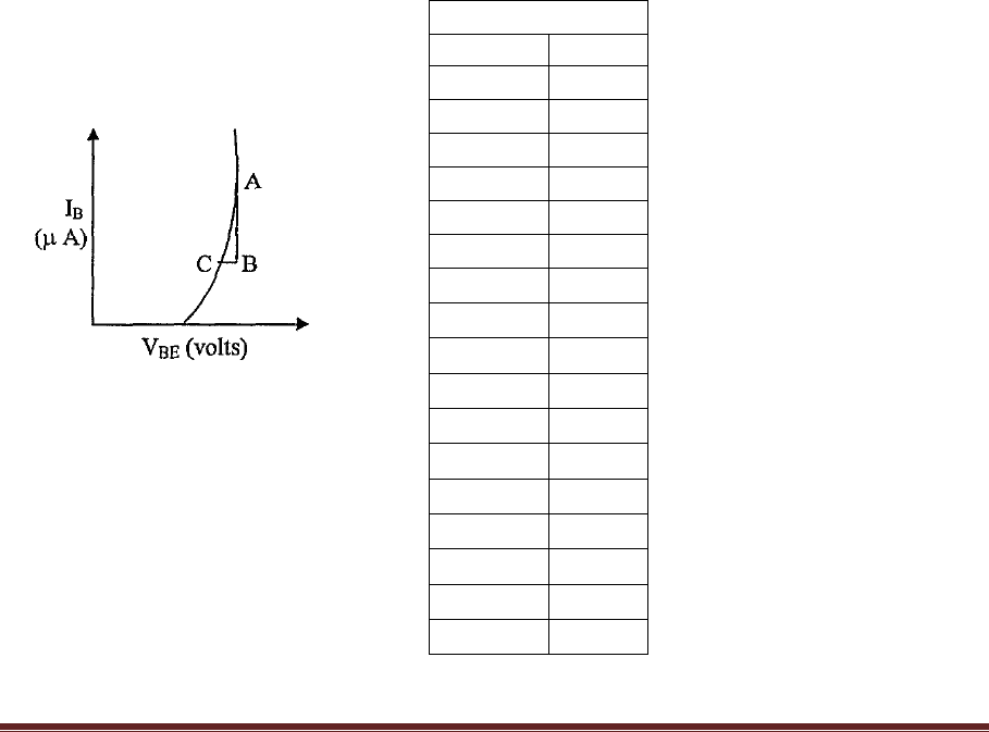
along Y- axis is plotted. Slope of the curve is
found in active region of transistor which is (i.e. linear portion of the curve) the
reciprocal of the input resistance values.
Output characteristics:
To study the output characteristics of the transistor. Again turn all the power
supply knobs to minimum position. Now the Base current I
B
is set to 25 μA by
turning V
BB
knob. Keeping I
B
=25 μA, apply V
CE
values as 0.2, 0.4, 0.6, 0.8 volts
till 1 volt and note down corresponding I
C
values. Tabulate all the values in
relevant tabular column for output characteristics. Care should be taken that while
taking each reading of Ic, I
B
should read the constant values i.e. I
B
=25 μA.
Now a graph of V
CE
along X-axis and Ic along Y-axis is plotted. Slope of the
curve is found in the active region of the transistor (i.e. linear portion of the
curve). Reciprocal of slope is the ratio ΔV
CE
/ ΔIc, and hence the output resistance
value.
Transfer characteristics:
To study the Transfer characteristics of the transistor. Turn all the power supply knobs
to minimum position again. Now set the collector-Emitter voltage V
CE
= 2 volt.
Apply I
B
values as 25 μA, 50 μA, 75 μA & 100 μA & note the Ic values in milli
amperes each time. Tabulate the readings in relevant tabular column for transfer
characteristics.
A graph of I
B
along X-axis & Ic along Y-axis is plotted. The graph obtained will be a
straight line, calculate the slope and slope will be the ratio ΔI
C
/ ΔI
B
, and hence the
current gain β values.
OBSERVATIONS:
Input characteristics:
V
CE
= 2V
V
BE
(mV)
I
B
(µA)
0
0
5

BMSIT&M Department of Physics Engineering Physics Lab manual August-2020
Page 11
Output characteristics:
I
B
=25 A
I
c
(mA)
V
CE
(volts)
Note: For Input characteristic triangle form should be small & it should be taken in the
linear portion of the curve
Transfer characteristics:
A
I
c
(mA)
C B
I
B
( A)
RESULT:
1. The input resistance = R
i
= ---------------- Ω
2. Current gain factor = β = -----------------
I
B
= 25 A
V
CE
(V)
I
C
(mA)
0
0.2
0.4
0.6
0.8
1.0
V
CE
=2 volt
I
B
(A)
I
C
(mA)
10
20
30
40
50
60
70
80
90
100

BMSIT&M Department of Physics Engineering Physics Lab manual August-2020
Page 12
3. DETERMINATION OF FERMI ENERGY
AIM: Determination of Fermi energy of copper using a Wheatstone metre bridge.
APPARATUS: Copper coil, standard resistance box, Metre Bridge, hot water, thermometer.
PRINCIPLE: Fermi energy is the energy of the electron at the highest occupied energy level
at absolute zero Kelvin
FORMULA:
19
2
2
22
F
106.1
1
ΔT
ΔR
x
2mL
πArne
E
x
x
(eV) …….(1)
Where
n is the free electron concentration in m
-3
,
e is the charge of electron in C,
A is the metal constant in mK,
r is radius of the coil in m,
L is the length of the copper wire in m,
m is the mass of electron in kg and
ΔT
ΔR
is the slope of the straight line obtained by plotting resistance of the copper coil
against absolute temperature in Ω/K.
E
F
is the Fermi energy in joule
PROCEDURE:
1. A copper coil which is wound on a wooden bar is immersed in hot water taken in a beaker.
A thermometer is also immersed in the beaker to note the temperature of water. The two ends
of the coil are connected to the left gap of a metre bridge.
2. A shunt resistance of 1Ω is connected in the right gap. The circuit is completed as shown
in the circuit diagram.
3. The water is allowed to cool and the balancing length is noted for every 5
0
C decrease in
temperature starting from 80
o
C.
4. The readings are tabulated and the resistance of the coil at various temperatures is
calculated.
5. A graph of resistance against absolute temperature is plotted which will be a straight line
(as shown in figure) and the slope is determined.
6. The slope is substituted in equation (1), the Fermi energy is calculated and also it is
expressed in eV.
OBSERVATIONS:
Length of the copper wire, L = 4m, Radius, r = 0.12x10
-3
m.
Metal Constant, A = λ
F
T= 2.32x10
-8
x 318 = 7.4x10
-6
mK.
Free electron concentration, n = 8.464x10
28
/m
3
.
Mass of electron, m = 9.1x10
-31
kg.
Charge of an electron, e = 1.6x10
-19
C

BMSIT&M Department of Physics Engineering Physics Lab manual August-2020
Page 13
CIRCUIT DIAGRAM:
Th
+
S
G
-
A B
--------------- L --------------------------------------(100 –L) -----------------------
+ -
Battery
TABULAR COLUMN:
Graph :
A
dR
C dT B
R (Ω)
T (K)
RESULT: The Fermi energy of copper is found to be ___________ eV.
Trials
Temp.
(C)
Temp.
(K)
Balancing length
‘ L’(cm)
Resistance
(100 )
SxL
R
L
(Ω)
1
80
353
75
348
2
70
343
65
338
3
60
333
4
55
328
5
50
323

BMSIT&M Department of Physics Engineering Physics Lab manual August-2020
Page 14
4. VERIFICATION OF SERIES AND PARALLEL RESONANCE
USING L. C. R. CIRCUITS.
AIM: To study the frequency response of the given series and parallel resonance circuits,
and hence to determine the inductance value of the unknown inductor, also to determine the
bandwidth and quality factor of the circuit in series resonance.
APPARATUS: Audio frequency oscillator, a c milliammeter, standard inductance coil,
standard resistors and capacitors, patch cards, etc.
PRINCIPLE: This experiment is based on the principle of resonance in AC electrical
circuits. An LCR circuit is essentially an oscillator; therefore it will have a definite natural
frequency depending on the value of L & C when the natural frequency of the LCR matches
with applied frequency supplied by the signal generator resonance takes place. In the case of
series LCR the current at resonance will be maximum, and in the case of parallel LCR current
at resonance will be minimum. A series LCR will be used as a tuning circuit and the parallel
circuit will be used as a filter circuit
CIRCUIT DIAGRAM:
Choose L = L
1,
R = 750Ω & C = 0.01μF
SERIES RESONANCE PARALLEL RESONANCE
(fig. a) (fig. b)
FORMULA: The unknown Inductance L is given by the formula
1.
22
1
4
r
L
fC
(H)
Where f
r
= Resonant frequency (Hz)
C = Capacitor value of the given LCR circuit. (μF)
The Band width of the given series LCR circuit is given by 2. Δf = f
2
-f
1
(Hz)
Where f
1
and f
2
are lower and upper cutoff frequencies
Quality factor Q is given by 3.
r
f
Q
f
PROCEDURE: SERIES RESONANCE
Connect the components, inductance L = L
1,
Resistance R = 750Ω, Capacitance C =
0.01μF in series and the function generator as shown in the circuit diagram. Initially
the circuit should be closed by switching on the power supply. The amplitude in the

BMSIT&M Department of Physics Engineering Physics Lab manual August-2020
Page 15
signal generator is adjusted for an optimum value and the signal generator should be
adjusted for sinusoidal mode. The frequency in the signal generator is set to 1 KHz.
The frequency is varied in steps of 500 Hz up to 4000 Hz, then insteps of 100 Hz
from 4000 Hz to 5500 Hz, then in steps of 500 Hz till 8000 Hz and the corresponding
current for each frequency is noted down. At a particular frequency we observe that,
the current in circuit becomes maximum and this frequency is called resonant
frequency (f
r
).
A graph is plotted between current and the frequency and the curve obtained is called
the frequency response curve of the given series LCR circuit. The bandwidth of the
LCR circuit gives us the measure of appropriate frequencies, which the given circuit
can pick up when used as a tuning circuit. The band width can be calculated as
follows: in the frequency response curve at a value of current equal to Imax/ √2 a
straight line parallel to frequency axis is drawn which cuts the curve at points A & B,
the frequencies corresponding to A&B are called f
1
& f
2
respectively. The difference
in f
2
& f
l
is called bandwidth. The quality factor Q gives us the sharpness of the
resonance curve which is given by the ratio of resonant frequency (f
r
) to band width
(Δf)
PARALLEL RESONANCE:
The circuit is connected as shown in the circuit diagram. The amplitude adjusted for
series resonance should be kept constant. The frequency is varied from1KHz to 8
KHz as before and the corresponding current is noted down in the milli ammeter. In
this case we observe that the current in the circuit gradually decreases in the
beginning and reaches a minimum value at resonance. The frequency corresponding
to minimum current in the circuit is called resonant frequency of the given parallel
LCR.
Since we are using same value of Inductance (L) and Capacitance (C) for both series
and parallel LCR circuit the value of resonant frequency in both cases should match.
A plot between current and the frequency is drawn as follows.

BMSIT&M Department of Physics Engineering Physics Lab manual August-2020
Page 16
I
(mA)
f
r
f (Hz)
TABULAR COLUMN: Choose L = L1, R = 750Ω & C = 0.01μF
Series LCR circuit
Parallel LCR circuit
Frequency (Hz)
Current (mA)
Frequency (Hz)
Current (mA)
1000
1000
1500
1500
2000
2000
2500
2500
3000
3000
3500
3500
4000
4000
4100
4100
4200
4200
4300
4300
4400
4400
4500
4500
4600
4600
4700
4700
4800
4800
4900
4900
5000
5000
5100
5100
5200
5200
5300
5300
5400
5400
5500
5500
6000
6000
6500
6500
7000
7000
7500
7500
8000
8000

BMSIT&M Department of Physics Engineering Physics Lab manual August-2020
Page 17
Calculations:
RESULT: The frequency response curve is studied, the values of
Series Resonant frequency = …………………….Hz
Unknown Inductance = ………………………….H
Bandwidth= ……………………………………...Hz
Quality factor =…………………………………...
Parallel resonant frequency = ……………………Hz
Note: Experiment can be repeated for different values of inductance ‘L’ and capacitor
‘C’ accordingly the range of frequencies must be selected.

BMSIT&M Department of Physics Engineering Physics Lab manual August-2020
Page 18
5. NEWTON’S RINGS
AIM: To determine the radius of curvature of a given Plano convex lens by Newton’s rings
method.
APPARATUS: Plano convex lens, Plane glass plate, Stand with a turn able glass plate,
traveling microscope, sodium vapour lamp etc.
PRINCIPLE: This experiment is based on the principle of interference of light in thin films.
In this experiment an air film is formed between a ground glass plate and a plano convex
lens. When a monochromatic light is made to incident on the combination of a Plano convex
lens and the remaining portion of light passes through Plano convex lens and gets reflected
from the bottom ground glass plate, these two components of light undergo interference to
form Newton’s Rings.
FORMULA: The radius of curvature of the curved surface of the lens is given by
22
4( )
mn
DD
R
mn
(m)
Where,
R= radius of curvature of the Plano convex lens in m.
D
m
= diameter of the m
th
dark ring in m.
D
n
= diameter of the n
th
dark ring in m.
= Wavelength of sodium light i.e., 5893 x10
-10
m.
FIGURE:
PROCEDURE:
Initially the Plano convex lens is tested to find out the curved surface of and the plane
surface which is done as follows. The Plano convex lens is placed on the ground glass
plate and it is rotated gently, if the lens rotates freely then the curved surface is facing
the ground glass otherwise due to friction the rotation will not be smooth in which
case the plane surface of the lens is in contact of the ground glass plate. Now we
1
st
dark ring
Zeroth dark ring
2
nd
dark ring

BMSIT&M Department of Physics Engineering Physics Lab manual August-2020
Page 19
should place the curved surface towards the ground glass plate, care should be taken
to see that there are no dust particles on both the surface of the lens and the surfaces
of the ground glass plate.
Now the reflector plate is adjusted until the intensity of light in the eyepiece becomes
maximum. When the intensity of the light is maximum the reflector plate will be at an
angle of 45
0
to the horizontal, later the focusing screw of the traveling microscope is
adjusted until the fringe patterns are seen. Initially the center of the fringe pattern may
not appear, and then the traveling microscope is aligned such that the intersection of
the cross wires coincide with the centre of the fringe pattern.
In an ideal Newton’s Ring set up there will be a central dark spot which corresponds
to the zeroeth ring of the system, in case if the central dark spot is not present the
inner most ring should be taken as ring no 1, initially the vertical cross wire of the
traveling microscope should be taken tangentially to 12
th
dark ring, therefore 12 rings
should be counted carefully towards left of the centre and the vertical cross wire
should be moved gradually tangential to the outer portion of the 12
th
ring, this is the
starting point of the experiment. The reading corresponding to the 12
th
dark ring is
noted down and tabulated in the given tabular column.
Later the vertical cross wire should be moved towards the centre and it should be
made coinciding with 10
th
dark ring and the reading for the 10
th
dark ring is noted.
Similarly readings of 8
th
, 6
th
, 4
th
and 2
nd
dark ring of the left hand side are noted down
by adjusting the vertical cross wire tangential to the respective rings. When the cross
wire reaches 2
nd
dark ring the counting of the rings can be verified. If the initial
counting of rings is correct then the cross wire will be exactly at two rings away from
the dark spot, otherwise either it will be ahead of the 2
nd
dark ring or behind the 2
nd
dark ring.
Now the cross wire should be moved towards RHS (right side) of the ring pattern. On
the right side readings should be taken in the ascending manner i.e. in the order 2, 4, -
--10 & 12 in this manner every ring will have a LHS reading and RHS reading.
The difference between the two will give us the diameter of the respective ring, thus
diameter of 12
th
, 10
th
& 8
th
are calculated and tabulated under the column D
m
.
Similarly diameters of 6
th
, 4
th
& 2
nd
rings are calculated and tabulated under the
column D
n
.
The values of D
m
2
and D
n
2
are separately determined and finally the value of (D
m
2
-
D
n
2
) is determined in each case. As per the theory of the Newton’s ring the value of
(D
m
2
- D
n
2
) in each case should be a constant. Therefore mean value of (D
m
2
- D
n
2
) is
found out and radius of curvature (R) of the Plano convex lens can be determined by
using the given formula.
22
()
4( )
m n mean
DD
R
mn
(m)

BMSIT&M Department of Physics Engineering Physics Lab manual August-2020
Page 20
OBSERVATIONS:
Least count of Screw gauge type traveling microscope:
Distance moved on pitch scale on n rotations
Pitch of screw gauge = ------------------------------------------------------------
No of rotations given to head scale (n)
Pitch = ………… mm
Pitch
L.C = -----------------------------------------------------------
No. of divisions on the head scale
L.C = ………….mm
TABULAR COLUMN:
Split readings:
Ring No.
PSR (mm)
HSR
TR= PSR+(HSRxLC)
(mm)
LHS 12
10
8
6
4
2
RHS 2
4
6
8
10
12

BMSIT&M Department of Physics Engineering Physics Lab manual August-2020
Page 21
To determine D
m
2
– D
n
2
:
Ring
No
‘m’
TM reading
(mm)
Diameter
D
m
= L
m
-R
m
(mm)
D
m
2
(mm
2
)
Ring
No
‘n’
TM reading
(mm)
Diameter
D
n
= L
n
-R
n
(mm)
D
n
2
(mm
2
)
D
m
2
– D
n
2
(mm
2
)
Left
L
m
Right
R
m
Left
L
n
Right
R
n
12.
10.
8.
6.
4.
2.
Mean (D
m
2
– D
n
2
) = …………….mm
2
= …………… x 10
-6
m
2
Calculations:
RESULT: The radius of curvature of the given Plano-convex lens R = ………m.
PRECAUTIONS:
1. While adjusting for the ring pattern care should be taken to see that the centre portion
of the Plano convex lens is right below the objective lens of traveling microscope.
2. While taking readings the cross wire should always be tangential to outer portion of
the ring.
BMSIT&M Department of Physics Engineering Physics Lab manual August-2020
Page 22
6. YOUNG’S MODULUS BY SINGLE CANTILEVER
AIM: - To determine the young’s modulus of the material of the given beam by the method
of single cantilever.
APPARATUS: - Single cantilever setup, slotted weights, travelling microscope, reading lens
and lamp.
PRINCIPLE: The experiment is based on the theory of bending moment of beams. .
Bending moment of a beam depends on the following factors:
a) Young’s modulus of the material of the beam
b) The cross section geometry of the beam
FORMULA:
3
3
4
bd
Mgl
Y
N/m
2
where, M – mass for which depression is found (in kg).
g - acceleration due to gravity (= 9.8 ms
-2
).
l - distance between the needle and fixed end (in m).
b & d - breadth and thickness of the wooden scale (in m).
- mean elevation produced (in m).
DIAGRAM:
Fig.1 Single cantilever
PROCEDURE:-
• The tip of the needle (inverted image) on the single cantilever is made to coincide with the
intersection of the cross wire of the travelling microscope (with no load in the hook).
• Note down the readings of the travelling microscope in the tabular column as the dead load
reading (ie. x g).
• Now add some weight to the hook (say 20 g). Again coincide the tip of the needle to the
intersection of the cross wire and corresponding readings are noted in the tabular column.

BMSIT&M Department of Physics Engineering Physics Lab manual August-2020
Page 23
• This is repeated up to 100 g in steps of 20 g every time and corresponding readings are
noted in the tabular column.
• The experiment is repeated by decreasing the load in the weight hanger in steps of 20 g and
the corresponding readings are taken and are tabulated.
• The depression or deflection of the cantilever beam ‘’, for load ‘M’ in kg is found out from
the tabular column.
• By using the breadth (b) and thickness (d) of the bar, the young’s modulus of the material of
the beam is calculated.
Precaution:
1. The pin has to be vertical before focusing
2. The beam must be parallel to horizontal scale of travelling microscope
Least count of travelling microscope:
LC = Value of 1MSD - Value of 1VSD ( or) LC= Value of 1MSD/Number of VSD
TR= MSR+ (CVD x LC)
BMSIT&M Department of Physics Engineering Physics Lab manual August- 2020
Page 24
Tabular column to find elevation
Load in
hanger
(g)
Load increasing
Load decreasing
Mean
R1
(cm)
Load
in
hanger
(g)
Load increasing
Load decreasing
Mean
R2
(cm)
Depression
= R1~R2
(cm)
MSR
(cm)
CVD
TR
(cm)
MSR
(cm)
CVD
TR
(cm)
MSR
(cm)
CVD
TR
(cm)
MSR
(cm)
CVD
TR
(cm)
X+0
X+60
X+20
X+80
X+40
X+100
Mean depression, = -----------x10
-2
m
CALCULATION:
3
3
4
bd
Mgl
Y
N/m
2
RESULT:-Young’s modulus of the material of the beam is found to be Y= -------------N/m
2
BMSIT&M Department of Physics Engineering Physics Lab manual August- 2020
Page 25
7. DETERMINATION OF DIELECTRIC CONSTANT BY
CHARGING AND DISCHARGING METHOD
AIM: To determine the dielectric constant of the given dielectric material by the method of
charging and discharging.
APPARATUS: Capacitor, Resistor, Two way toggle switch, Voltmeter, stop watch.
FORMUIA: Dielectric constant of a given material is given by
AR
dT
K
0
6
2
1
693.0
10
Where, K = Dielectric constant of the material
T
1/2
= Time taken by the capacitor for half charging / discharging in S.
d = Distance between the two plates = m.
Є
0
= Permittivity of free space = 8.852 x 10
-12
F/ m
A = Area of the capacitor plate = m
2
.
R = Resistance = .
[ Constans for Kit-1: A = 47x5x10
-6
m
2
, C = 0.01μF, d = 0.075x10
-3
m, R = 100 kΩ]
[ Constants for kit-2: A = 120x6x10
-6
m
2
, C = 220μF, d = 0.1x10
-3
m, R = 100 kΩ]
CIRCUIT DIAGRAM:
+
V Discharging
+
R C Charging
+ -
Battery
PROCEDURE:
Make the connections as shown in the circuit diagram
The capacitor is allowed to charge by switching the toggle switch to the position 1and
simultaneously a stop watch is started.
The voltage across the capacitor is noted down at an interval of 5 second using a stop
watch and the readings are entered in the tabular column.

BMSIT&M Department of Physics Engineering Physics Lab manual August- 2020
Page 26
Now the stop watch is reset, the capacitor is allowed to discharge by switching the toggle
switch to the position 2 and simultaneously stopwatch is started, the voltage across the
capacitor is noted down for the same interval of time.
A graph of t along X-axis and V along Y-axis is plotted for both charging and
discharging as shown in the sketch of the graph.
The time (T
1/2
) corresponding to the intersection of the two curves is noted.
The dielectric constant of the material is calculated by substituting the value of T
1/2
in the
given formula.
TABULAR COLUMN:
CHARGING DISCHARGING
Time ‘t’
in second
Voltage ‘V’
in volts
Time ‘t’
in second
Voltage ‘V’
in volts
0
0
0
5
5
10
10
15
15
20
20
25
25
30
30
35
35
40
40
45
45
50
50
55
55
60
60
GRAPH:
Charging curve
V
in volts
Discharging curve
t = T
1/2
t in seconds
RESULT: Dielectric constant (K) of the given material is found to be ---------------------

BMSIT&M Department of Physics Engineering Physics Lab manual August- 2020
Page 27
8. WAVELENGTH OF LASER LIGHT USING A SEMICONDUCTOR
LASER
AIM: To determine the wavelength of laser light by diffraction technique using a plane
diffraction grating.
APPARATUS: Semiconductor diode laser source, grating with holder, scale, screen.
PRINCIPLE: Diffraction of light occurs when the width of the obstacle is comparable to the
wavelength of the light source. The light from the laser source is allowed to fall normally on the
grating, by measuring the distance between the diffracted spots, the wavelength of laser light is
determined.
FORMULA:
sin
m
d
m
nm
Where = Wavelength of laser light measured in m
d = Grating constant measured in m
Example:- For 100 number of lines per mm of a grating ‘d’ can be calculated as below
md
m/ linesofNumber
1
m = difference between the order of spots
1
tan
m
m
x
R
m
= angle of diffraction for m
th
order spot
X
m
= distance between Zero
th
order spot and m
th
order spot measured in m
R = distance between screen and grating measured in m
DIAGRAM:
0
I
I
II
II
BMSIT&M Department of Physics Engineering Physics Lab manual August- 2020
Page 28
Procedure:
1. Place the grating in its holder and the screen is placed at a distance of R cm as mentioned
in the tabular column.
2. The grating is kept between the laser source and the screen.
3. Laser beam undergoes diffraction after passing through the grating. The diffraction spots
are observed on the screen.
4. The distances 2x
m
between the symmetrical spots on either side of central bright spot are
measured and recorded.
5. The angle of diffraction
m
is calculated using
1
tan
m
m
x
R
.
6. is calculated using the formula
sin
m
d
m
.
TABULAR COLUMN.
Trial
No.
R
(In cm)
Order of
the
diffraction
pattern
(m)
2x
m
(in cm)
x
m
(in cm)
1
tan
m
m
x
R
sin
m
d
m
(in m)
1
80
1
2
2
3
3
4
4
5
5
1
90
1
2
2
3
3
4
4
5
5
av
= …………………. m
CALCULATIONS:
RESULT:- The wavelength of the given laser light source is: ………………..nm.

BMSIT&M Department of Physics Engineering Physics Lab manual August- 2020
Page 29
9. NUMERICAL APERTURE
AIM: To determine the Acceptance angle and Numerical aperture of the given optical fiber.
APPARATUS: Laser source, Optical fiber, Screen, Scale.
PRINCIPLE: The Sine of the acceptance angle of an optical fiber is known as the numerical
aperture of the fiber. The acceptance angle can also be measured as the angle spread by the light
signal at the emerging end of the optical fiber. Therefore, by measuring the diameter of the light
spot on a screen and by knowing the distance from the fiber end to the screen, we can measure
the acceptance angle and there by the numerical aperture of the fiber.
FORMULA: The Acceptance angle,
L
D
2
tan
1
0
Where D – the diameter of the bright circle formed on screen,
L – the distance between the optical fiber end and screen.
And the Numerical Aperture,
0
sin
NA
DIAGRAM:
PROCEDURE:
Switch on the laser source and adjust the distance between output end of the optical fiber
and the screen ‘L’ (say 2 cm).
Place a graph sheet on the screen and observe the circle formed on the graph sheet.
Mark the points ‘a’,’b’,’c’ & ‘d’ on the inner bright circle as shown in the diagram. Note
down the horizontal diameter D
1
and vertical diameter D
2
of the inner bright circle in the
tabular column.
Repeat the above steps for different values of L (for 4cm, 6cm, … ).
Find the Acceptance angle from the tabular column and hence the Numerical aperture.
a
b
c d
L
Optical fiber cable
Laser source
Screen

BMSIT&M Department of Physics Engineering Physics Lab manual August- 2020
Page 30
Tabular column:
Trail
No.
L
(in
cm)
Horizontal
diameter D
1
(in cm)
Vertical
diameter D
2
(in cm)
Mean
Diameter D
(in cm)
Acceptance
angle
L
D
2
tan
1
0
Numerical
aperture NA
0
sin
NA
1
2
2
4
3
6
4
8
5
10
mean
mean
NA
0
CALCULATIONS:
RESULT: The Angle of acceptance and Numerical aperture of the given optical fiber are found
to be
0
=
NA =
Note:
The source of error in this experiment is, marking of the dark circle. The diameter
markings should be done only on the inner dark circle, not for the outer circle. Refer
the diagram given above for correct markings. Error in this part would be more as it
depends on the eye sensitivity of the observer also.
Avoid staring at the light spot for longer times, as it will strain the eye quickly.
Do not view the laser light directly from source as it may damage eye permanently
Do not bend the fiber with sharp bending curvatures as it may damage the fiber
permanently. Do not touch the fiber end points with bare hands as it may contaminate the
fiber open end surface and it may degrade the output quality.

BMSIT&M Department of Physics Engineering Physics Lab manual August- 2020
Page 31
10. DETERMINATION OF SPRING CONSTANT
AIM: a) To determine spring constant for the material of the given spring and b) To determine
Spring constant in series and parallel combination.
APPARATUS: Given springs, slotted weights
PRINCIPLE: Elastic materials are those which retain their original dimensions after the
removal of deforming forces. Application of a force on a spring causes elongation. When
subjected to stress, strain is produced. Within the elastic limit, the ratio of stress to strain is a
constant known as modulus of elasticity. The restoring force is always directed opposite to
displacement.
Restoring force α – displacement
F = -K x (N)
Here “k” is the proportionality constant known as spring constant. It is a relative measure of
stiffness of the material.
Formula: (1) Spring constant K = - F/x (N/m)
(2) Spring constant in series combination (N/m)
(3) Spring constant in parallel combination (N/m)
PROCEDURE:
1. Connect the given spring to a rigid support.
2. Attach the weight hanger (dead load) to the end of the spring and note down the initial
displacement “a” produced on the scale.
3. Increase the weight in steps of 50 g and note down the displacement (b) produced in the
spring. Find the elongation x= (b-a) . Using the formula (1) find spring constant K
1
.
4. Repeat the above steps and find spring constant K
2
for the second spring.
5. Connect the two springs in series combination and repeat the above procedure to find k
series.
6. Connect the two springs in parallel combination and repeat the above procedure to find k
parallel
.
7. Compare the experimental results obtained with the theoretical value.

BMSIT&M Department of Physics Engineering Physics Lab manual August- 2020
Page 32
Tabular column:
Determination of spring constant for spring 1
Displacement for the initial load (W+0) a = …..cm.
Tr. no
Mass
m (g )
F =
mg
(N)
Displacement
b (cm)
Elongation
∆X= (b-a)
(cm)
Spring
constant K
1
(N/m)
1
W+50
2
W+100
3
W+150
4
W+200
Average K
1= ………………….N/m
Determination of spring constant for spring 2
Displacement for dead load (W+0) a = …..cm.
Tr. no
Mass
m (g )
F =
mg
(N)
Displacement
b (cm)
Elongation
∆X=(b-a)
(cm)
Spring constant
K
2
(N/m)
1
W+50
2
W+100
3
W+150
4
W+200
Average K
2= ………………….N/m
Determination of spring constant in series combination
Displacement for dead load (W+0) a = …..cm
Tr. no
Mass
m (g )
F =
mg
(N)
Displacement
b (cm)
Elongation
∆X= (b-a)
(cm)
Spring
constant K
series
(N/m)
1
W+50
2
W+100
3
W+150
4
W+200
Average K
series= ………………….N/m

BMSIT&M Department of Physics Engineering Physics Lab manual August- 2020
Page 33
Determination of spring constant in parallel combination
Displacement for dead load (W+0) a = …..cm
Tr. no
Mass
m (g )
F =
mg
(N)
Displacement
b (cm)
Elongation
∆X= (b-a)
(cm)
Spring
constant
K
parallel
(N/m)
1
W+50
2
W+100
3
W+150
4
W+200
Average k
parallel= ………………….N/m
Diagrams:
Result:
1. The spring constant of the given material of the springs are found to be
K
1
=…………… N/m
K
2
……………. N/m.
2. Spring constants in series and parallel combinations are found to be
Combination
Theoretical (N/m)
Experimental (N/m)
Series
K
series
=
K
series
=
Parallel
k
parallel
=
k
parallel
=

BMSIT&M Department of Physics Engineering Physics Lab manual August- 2020
Page 34
11. CHARACTERISTICS OF PHOTODIODE
AIM: To study the reverse bias characteristics of the photodiode and hence to find the
Responsivity.
APPARATUS: Photodiode, Bulb, power supplies and Ammeter, micro ammeter, Voltmeters.
PRINCIPLE: Photodiode is a two terminal junction diode in which the reverse saturation
current changes when it’s reverse biased junction is illuminated by suitable wavelength of light.
This small amount of reverse saturation current is due to thermally generated electron-hole pairs.
The number of these minority charge carriers depends on the intensity of light incident on the
junction. When the diode is in a glass package, light can reach the junction and thus changes the
reverse current.
Formula: Responsivity of the Photo diode, R = slope of the graph ampere /watt
CIRCUIT DIAGRAM:
d=1cm
PROCEDURE:-
To study the reverse bias characteristics of the photodiode.
1) The electrical connections are made as shown in the circuit diagram;
2) The photo diode is moved towards the bulb and the distance between them is adjusted to
around 1cm.
3) The Power supplies are switched on and the voltage across the bulb is increased or the
distance between the bulb and the diode is adjusted till the micro ammeter reads photocurrent
of 3A.
4) For this fixed intensity of the bulb the reverse bias voltage across the photodiode varied as 1,
2, 3 and 4 volts and the corresponding micro ammeter reading is recorded in the tabular
column.
5) The experiment is repeated by varying the intensity of the bulb for 5A and 10A of photo
currents.
6) The graph is plotted between current versus voltage for different intensity of the bulb in the
third quadrant of the graph, because the current and voltages are for the reverse bias.
0 – 5V
Source
µ
A
Photo
diode
Bulb
0 – 15 V
Source
A
V
-
+
+
-
+
-
-
+
V
-
+

BMSIT&M Department of Physics Engineering Physics Lab manual August- 2020
Page 35
7) The characteristics of photodiode in reverse bias condition are obtained as shown in the
specimen graph.
To find the Responsivity of the photo diode
1) With the same electrical connections the distance between the diode and the filament of
the bulb is adjusted to 1cm.
2) The voltage across the bulb is adjusted to say 5V ( > 5V to get linear response) and the
corresponding current through the diode is noted in the second tabular column.
3) The voltage is increased in steps of 0.5V up to around 12V and the corresponding
currents through the photo diode are tabulated.
4) A graph of photo current v/s power is plotted and the Responsivity is calculated from the
slope of the curve.
Specimen graph:-
Photo diode reverse characteristics curves Photo diode Responsivity graph
For Low intensity of light
For Moderate intensity of light
For High intensity of light
0
10
20
30
Reverse
bias
current
in A
Reverse bias Voltage
in Volts
4V 3V 2V 1V
0V
0 0.5 1 1.5 2 2.5 3 3.5 4 4.5
60
50
40
30
20
10
Power in W
Current
in µA

BMSIT&M Department of Physics Engineering Physics Lab manual August- 2020
Page 36
OBSERVATIONS:
Reverse bias characteristics
Sl
No.
For various Intensity of the Bulb
Low intensity
Moderate intensity
High intensity
Biasing
voltage in
volts
Current(I)
in A
Biasing
voltage in
volts
Current (I)
in A
Biasing
voltage in
volts
Current (I)
in A
1
0
3
0
5
0
7
2
1
1
1
3
2
2
2
4
3
3
3
5
4
4
4
Power Responsivity
Radius of the photodiode, r = 2mm,
Distance from filament of the bulb to the photodiode, d = ……………. Cm (say 1cm)
Sl No.
Across the bulb
Power falling
on photodiode
2
2
4d
rP
P
o
Photodiode
Current in A
V in V
I in A
P
o
in W
1
5
2
5.5
3
6
4
6.5
5
7
6
7.5
7
8
8
8.5
9
9
Result: - The I-V characteristics of the given photodiode for different intensity of light is as
represented in the graph. From the graph it is clear that the reverse saturation current is
independent of biasing voltage and depends only on light intensity.
The Power Responsivity of the given photodiode is found to be, R =

BMSIT&M Department of Physics Engineering Physics Lab manual August- 2020
Page 37
12. Magnetic Intensity along the axis of a coil
AIM: To determine the magnetic field intensity along the axis of a circular coil carrying current
and earth’s horizontal magnetic field by deflection method.
APPARATUS: Deflection magnetometer, sprit level, commutator, ammeter, variable power
supply and connecting wires.
FORMULA:
2
3
22
2
0
2
xa
anI
B
(T)
Where B – the magnetic field intensity at the centre of a circular coil, (T)
n – Number of turns in the TG coil,
a – radius of the coil (cm)
x – Distance between the center of the coil and pointer in
the compass box
0
- Permeability of free space = 4πx10
-7
Hm
-1
.
I – the current through the coil (I)
tan
B
B
H
(T)
Where B
H
– horizontal component of earth’s magnetic field and
θ – mean deflection in TG.
CIRCUIT DIAGRAM:
PROCEDURE:
1. The connections are made as shown in the circuit diagram.
2. Arrange the deflection of the magnetometer in the magnetic meridian of the earth
3. Now align the plane of the coil with respect to 90°-90° line of the magnetometer.
4. Keep the magnetometer exactly at the centre of the coil (for this case x = 0).
5. Pass a current I (say 0.3 A) to flow through the coil and the corresponding magnetometer
deflections θ
1
and θ
2
are noted.
6. The direction of the current is reversed by using the commutator C and the corresponding
magnetometer deflections θ
3
and θ
4
are noted.
7. Average deflection θ is calculated.
A
C
x
BMSIT&M Department of Physics Engineering Physics Lab manual August- 2020
Page 38
8. Calculate the magnetic field at the centre of the coil by using the given formula
2
3
22
2
0
2
xa
a
nl
B
and also B
H
.
9. Repeat the experiment for different values of x (say 5cm, 10cm, …) by sliding the
magnetometer along the axis.
10. Find the average of both B and B
H
.
TABULOR COLUMN:
Radius of the coil, a = 8.2 cm and for n = 50 turns
Sl. No.
Current I
in A
X
in cm
Deflections in
degrees
Average θ
in degree
B
in x10
-5
T
tan
B
B
H
in x10
-6
T
θ
1
θ
2
θ
3
θ
4
1
0.3
0
2
5
3
10
1
0.4
0
2
5
3
10
Mean value of B
H
= ……………….(T)
Calculations:
Result: 1. Magnetic field at the center of the circular coil carrying current is found to be
(i) For current I= 0.3 A, B=…………………… T
(ii) For current I= 0.4 A, B=…………………… T
2. Earth’s horizontal magnetic field is found to be B
H
………………T.

BMSIT&M Department of Physics Engineering Physics Lab manual August- 2020
Page 39
VIVA QUESTIONS
1. TORSIONAL PENDULUM
1. What is torsional pendulum?
2. Define moment of inertia?
3. What are the factors which affects the moment of inertia?
4. Define rigidity modulus?
5. On what factors the rigidity modulus depends?
6. Explain the applications of torsional pendulum?
2. TRANSISTOR CHARACTERISTICS
1. What is a transistor?
2. What are input characteristics curves? What information we can get from input characteristics
curves?
3. Explain the terms depletion region, barrier potential.
4. What are the different configurations in which a transistor can be used in a circuit?
5. Define current gain.
6. What do you mean by doping?
7. Explain the mechanism of amplification in an NPN transistor under CE mode.
3. DETERMINATION OF FERMI ENRGY OF A METAL
1. Define the terms Fermi energy, Fermi velocity and Fermi temperature of a metal.
2. What is Fermi factor?
3. What is the probability of occupation at Fermi level for a temperature T≠0
0
K?
4. What are the factors which will influence the Fermi energy of the metal?
5. What is the average value of Fermi energy for metals?
4. SERIES AND PARALLEL RESONANCE
1. What are inductor, capacitor and resistor?
2. What are active and passive circuit elements?
3. What is resonance?
4. Why current is maximum at resonance in series resonance circuit?
5. Why current is minimum at resonance in parallel resonance circuit?
6. What is meant by quality factor?
7. What do you mean by sharpness of resonance?
5. NEWTON’S RINGS
1. What are Newton’s rings?
2. Why Newton’s rings are circular in shape.

BMSIT&M Department of Physics Engineering Physics Lab manual August- 2020
Page 40
3. Why the rings are observed only for an inclination of 45
0
of the glass plate to the incident
light.
4. Why the centre of the Newton’s rings in a reflected system of light is always dark.
5. What will be the effect on the ring system if we introduce water between the lens and the
glass?
6. What do you mean by radius of curvature?
6. YOUNG’S MODULUS
1. Define Young’s modulus.
2. How many types of stresses are there?
3. What is elasticity? Give an example for an elastic body.
4. Explain the terms stress, strain.
5. State Hook’s law.
6. What is a beam?
7. Give an example of elastic body and non-elastic body.
7. DIELECTRIC CONSTANT
1. What are dielectrics?
2. What is the role of dielectric in a capacitor?
3. What are the applications of dielectric materials?
4. What are the different types of dielectrics?
5. What is Static and Dynamic dielectric constant?
6. What is Polarization?
8. LASER DIFFRACTION
1. What kind of LASER light source is used in this experiment?
2. What is diffraction? State the condition to have proper diffraction.
3. State the principle of semiconductor diode laser?
4. Define stimulated emission, population inversion and metastable state?
5. List few applications of diode laser?
9. Numerical Aperture
1. What is the basic principle that can guide the signal through optical fiber?
2. Define Numerical aperture.
3. What is acceptance angle?
4. What are differences between Step Index and Graded index fibers?
5. What is V-number?
6. No. of guided modes through step index multimode fiber is ________

BMSIT&M Department of Physics Engineering Physics Lab manual August- 2020
Page 41
10. DETERMINATION OF SPRING CONSTANT
1. Define simple harmonic motion.
2. What are free vibrations?
3. Period of oscillation of a spring depends on what factors.
4. When two springs are connected in series what is the net spring constant?
5. When two springs are connected in parallel what is the net spring constant?
6. Define spring constant.
7. Mention the factors on which spring constant of a material depends.
11. PHOTO DIODE
1. What is a photo diode?
2. What is the difference between LED and photo diode?
3. What is the principle of operation of Photo diode?
4. What is responsivity?
5. What is dark current?
12. MAGNETIC FIELD ALONG THE AXIS OF A COIL
1. What is the principle involved in the experiment?
2. State Biot Savart’s law
3. Mention the factors on which magnetic field due to a circular coil carrying current depends.
4. What is the magnetic flux associated with a current carrying a circular coil of radius with?
current strength equal to I?
5. Define 1 weber.
********** ********** ********** ********** **********
